Technology & Innovation
At the core of INDNIX is an uncompromising commitment to process excellence. Our 35.40-acre Bengal Mega-Fab offers a comprehensive suite of semiconductor technologies engineered for automotive, telecommunications, and deeptech IoT.
Our Technology
Portfolio
From 28nm front-end silicon fabrication to advanced 3D packaging, explore our vertically integrated capabilities.
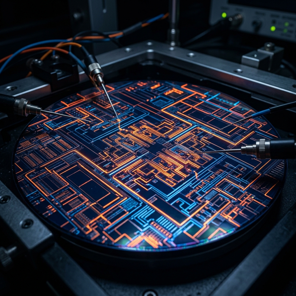
Process Nodes
28nm to 180nm+ capabilities across Analog, RF, BCD, and Power technologies for automotive, industrial, and IoT applications.
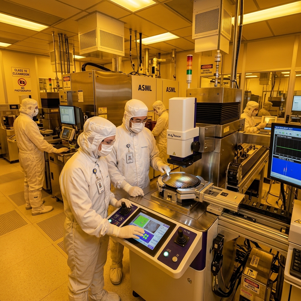
Compound & MEMS
III-V compound semiconductor and MEMS fabrication for optical, radar, and advanced sensing applications.
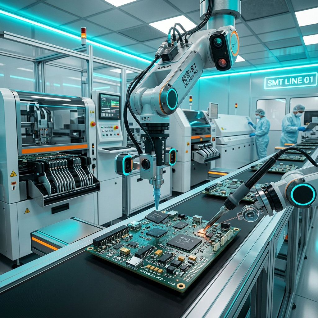
Advanced Packaging
SiP, Flip-Chip BGA, and Wafer-Level CSP solutions for high-density, mission-critical applications.
Quality & Reliability
AEC-Q100, ISO 9001, and IATF 16949 certified metrology, burn-in, and reliability testing.
EDA Ecosystem
Silicon-verified PDKs and IP libraries with Cadence, Synopsys, Siemens EDA, and Ansys partnerships.
Research & Development
Next-generation wide bandgap materials, advanced MEMS, and novel device architectures.
Ready to Start Your
Next Tapeout?
Our engineering team is ready to discuss your architecture, verify design rules, and recommend the optimal process node for your tapeout.