9 Integrated Divisions, One Campus
Assembly & Test, Compound Fab, RF, Power, Analog, IoT, Design, AI & Software — all under one roof.
Integrated Manufacturing Divisions
From compound wafer fabrication to full-scale OSAT capabilities.
MCUs & Logic
32-bit automotive-grade & IoT SoCs
Power Management
PMICs, DC-DC, LDOs for EV & Grid
Analog & Mixed-Signal
Precision ADCs, DACs, Op-Amps
Compound RF & MEMS
GHz-band devices & MEMS sensors
Finished Hardware
Complete PCBA modules
IP & Design Services
RTL-to-GDS ASIC Design
View All Technologies
Integrated Semiconductor Mega-Fab
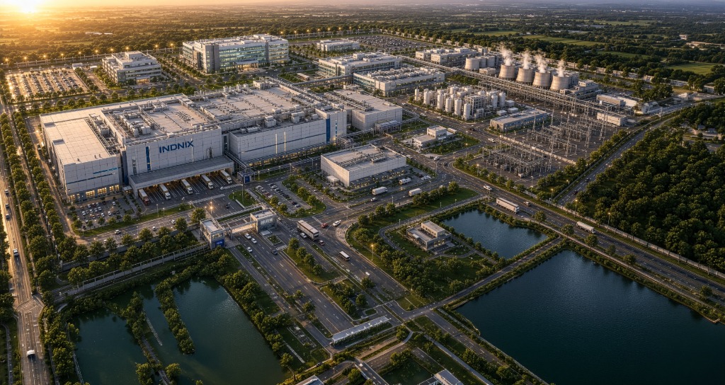
Eastern India’s first sovereign vertically integrated "Giga-Fab". Our highly secure 40.68-acre campus features a Stage 1 Target Capacity of 70,000 Wafer Starts Per Month (WSPM) across three heavily segregated manufacturing divisions.

Silicon Front-End Foundry
Our core revenue driver focusing on high-volume production of logic, analog, and PMICs. Built on massive concrete 'Waffle Slabs' for micro-seismic isolation.

Compound Semiconductor & MEMS Fab
Physically isolated cleanroom for exotic materials (GaAs, InP) preventing cross-contamination. Utilizes DRIE to carve microscopic cavities for MEMS sensors.
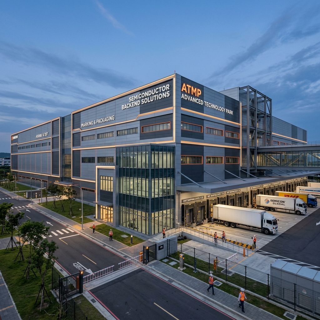
ATMP / SMT Backend Assembly
Captures value across the supply chain. Wafers are thinned, laser-diced, and packaged into finished, market-ready engine control units (ECUs) via PCBA.
Integrated Semiconductor Mega-Fab Complex
A state-of-the-art facility designed for advanced semiconductor manufacturing, assembly, testing, and research operations.
Facility Operations Showcase
Step inside our manufacturing lines. Explore the high-fidelity metrology logs, precision metrics, and cleanroom hardware powering our output.
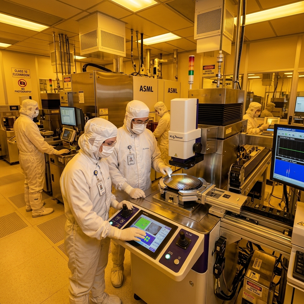
ISO Class 5 Cleanroom
Wafer fabrication cleanroom facility utilizing advanced ArF lithography systems and robotic wafer handling tracks.
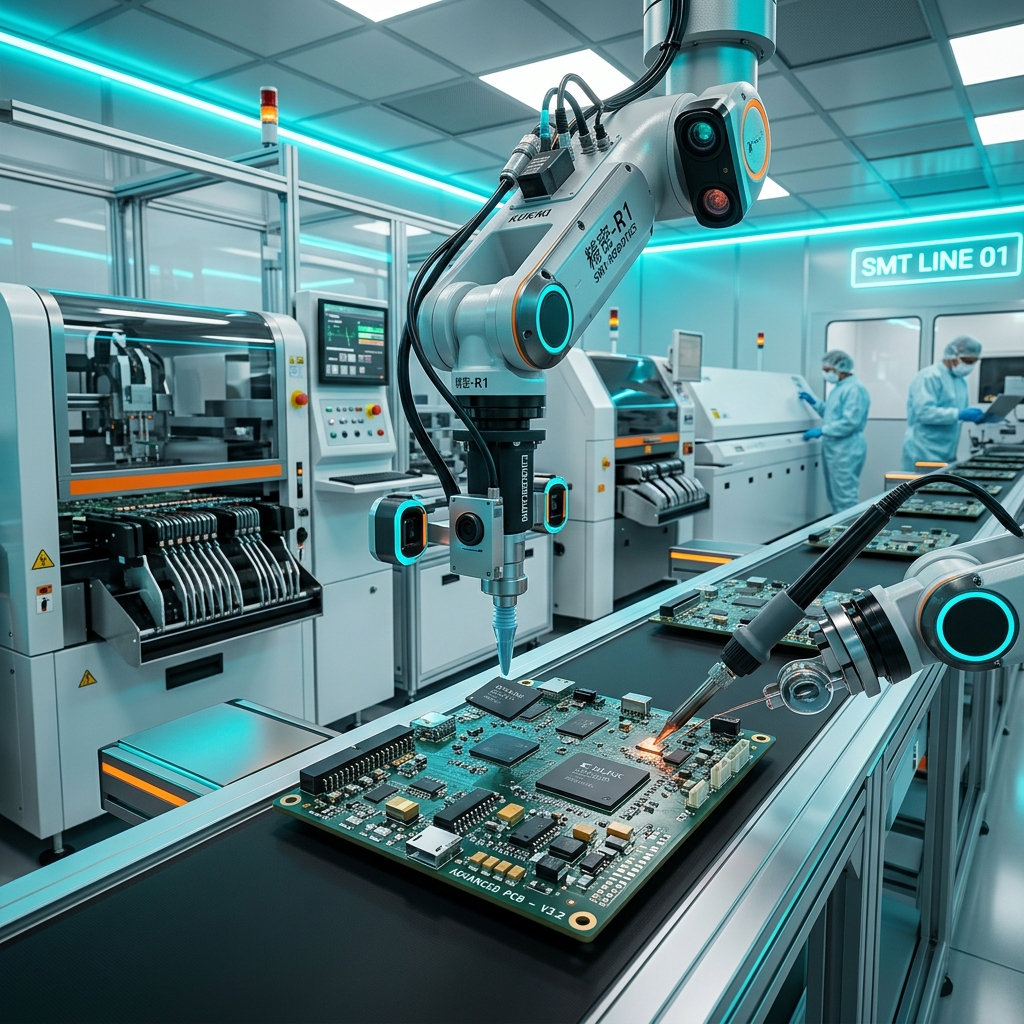
Robotic SMT Assembly Lines
High-speed surface mount technology placing microscopic components on motherboards with sub-micron precision.
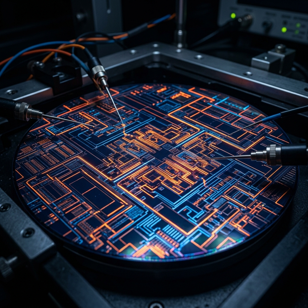
Wafer Probe Metrology
Macro silicon wafer testing under optical microscopes and ultra-fine probe cards to identify electrical node faults.
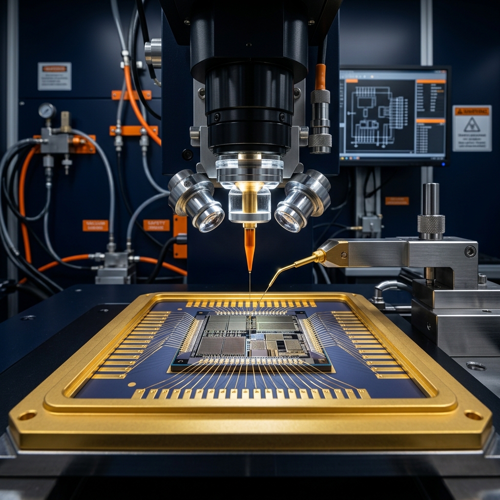
Advanced Chip Packaging
Microscopic wire-bonding micro-lenses attaching gold and copper wire traces to raw silicon core dies.
0+
0–180nm
0+
0 Acres
0/7
$0Billion
Technology Highlights
Cutting-edge semiconductor capabilities powering the next generation of global electronics.
Quality & Certification
Every wafer and assembled unit undergoes rigorous metrology, electrical testing, and reliability qualification — meeting ISO, IATF, and AEC-Q100 standards.
Certifications
ISO 9001, 14001, IATF 16949
Testing
Burn-in, HTOL, ESD
Defect Target
< 0.1 DPPM
Responsible Manufacturing for a Sustainable Future
Our commitment extends beyond silicon — water reclamation, renewable energy, and ethical supply chain practices are woven into every process.
Learn About Our Commitment85%
Water Reclamation
Recovery Target
40%
Renewable Energy
Power from Solar
90%
Waste Reduction
Recycling Rate
2035
Carbon Neutral
Net-Zero Target
Certifications & Affiliations
News & Insights
Latest technical articles, press releases, and industry perspectives from INDNIX.
INDNIX Proposes Mega-Fab to West Bengal State Government
INDNIX Technology Limited has proposed a comprehensive $1.5B USD mega-fab at the Bengal Silicon Valley Tech Hub, following a high-level meeting with State Government officials.
The Future of Advanced System-in-Package (SiP) Assembly
Explore how System-in-Package assembly is revolutionizing electronics by integrating multiple dies, passives, and sensors into a single compact module.
Overcoming Thermal Challenges in High-Density PCB Assembly
Learn the engineering strategies behind managing heat in densely populated PCB assemblies, from reflow profile optimization to advanced thermal interface materials.