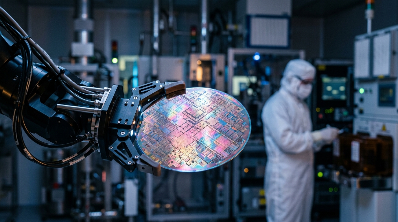
Engineering India's Semiconductor Future
From 28nm wafer fabrication to AI datacenter infrastructure — building sovereign silicon capability at Haringhata, West Bengal.
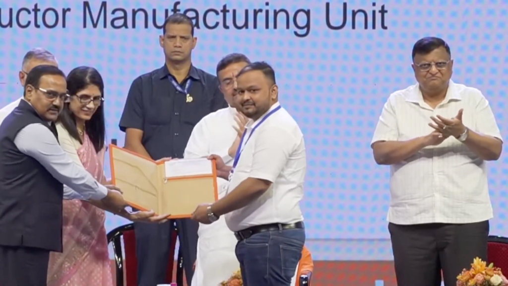
Soham Biswas, Chairman & MD
Receiving the Official Land Allotment Document for Semiconductor Manufacturing Unit at Milan Mela Prangan, Kolkata.
Land Allotted.
Mega-Fab Begins.
In a historic milestone for India's semiconductor sovereignty, the Government of West Bengal officially allotted land to INDNIX Technology Limited at the Haringhata Industrial Park, Nadia — formally handed over at the State Land Allotment Ceremony.
"Receiving land at Haringhata Industrial Park is not just a milestone — it is the moment INDNIX becomes real for Bengal and for India."
— Soham Biswas, Chairman & MDIntegrated Manufacturing
Capabilities
From 28nm silicon wafer fabrication to turnkey OSAT packaging — all vertically integrated on our sovereign 35.40-acre campus.
MCUs & Digital Logic
32-bit automotive-grade & IoT microcontrollers manufactured from 28nm to 180nm planar and FinFET CMOS.
Power Management & GaN
High-efficiency PMICs, DC-DC buck converters, and GaN/SiC power stages engineered for EV & grid infrastructure.
Analog & Mixed-Signal
Ultra-low noise ADCs, DACs, sensor interfaces, and precision operational amplifiers for aerospace and medical.
Compound RF & MEMS
Physically isolated cleanroom for GaAs and InP epitaxy, 5G/6G RF front-ends, and DRIE silicon micro-cavity MEMS.
OSAT & Turnkey Hardware
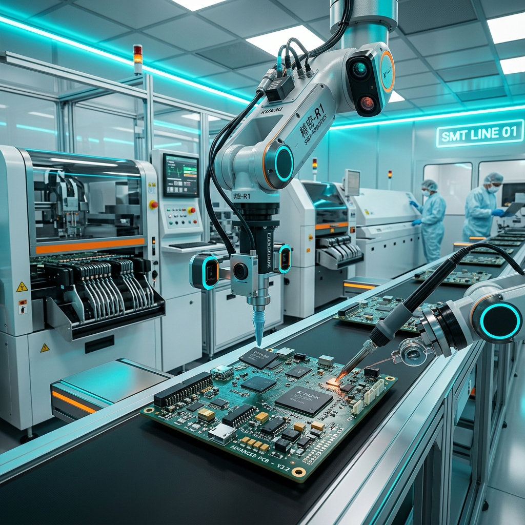
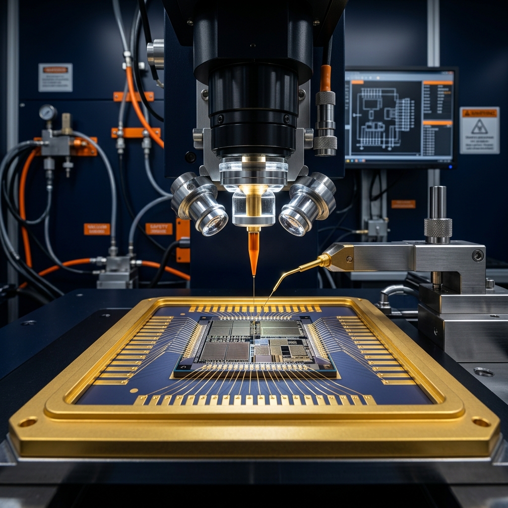
Advanced ATMP packaging with ultrasonic wire bonding, flip-chip SiP, and high-speed robotic SMT module lines.
ASIC Design & IP Licensing
Complete architectural RTL-to-GDSII ASIC design flow, foundry-certified PDKs, and pre-verified analog/digital IP blocks.
Empowering India's Next
Semiconductor Startups & Universities
INDNIX bridges the gap between deeptech innovation and high-volume commercial semiconductor manufacturing. We provide direct Class 1 cleanroom fabrication, Multi-Project Wafer (MPW) shuttles, and joint R&D for startups and academic institutions.
Semiconductor Startups
Direct access to commercial wafer foundry, verified PDKs, MPW shuttle slots, and turnkey OSAT packaging for your prototype chips.
Universities & Research Labs
Formal MoUs for sponsored cleanroom access, PhD scholar tool hours, student industrial internships, and joint patent development.
Integrated Semiconductor
Mega-Fab Complex
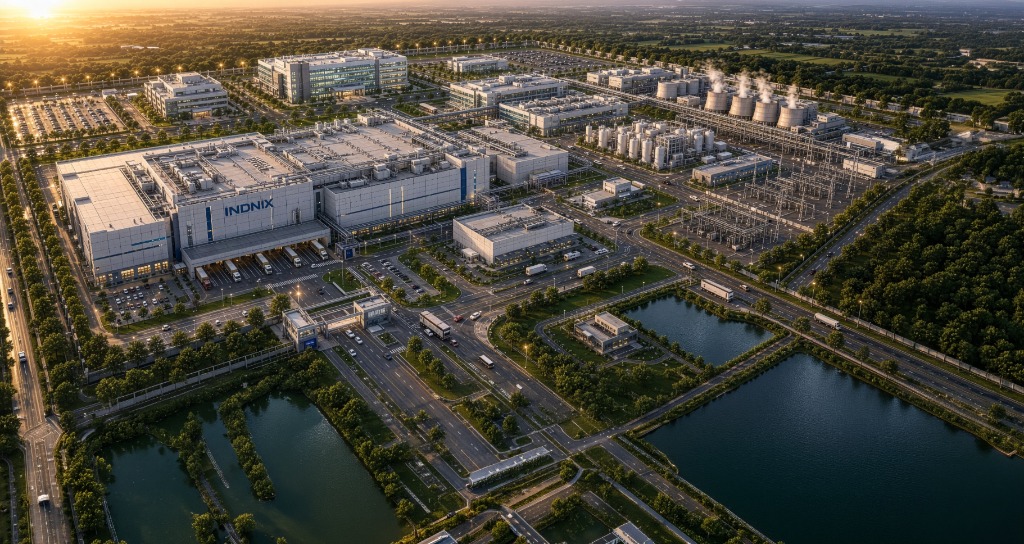
Eastern India’s first sovereign vertically integrated mega-fab. Our highly secure 35.40-acre campus features a Stage 1 Target Capacity of 70,000 Wafer Starts Per Month (WSPM) across three heavily segregated manufacturing divisions.
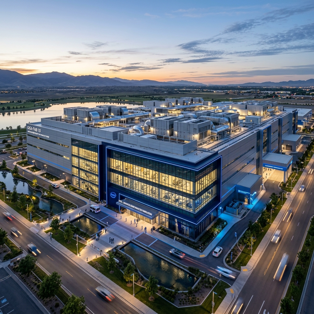
Silicon Front-End Foundry
Our core revenue driver focusing on high-volume production of logic, analog, and PMICs. Built on massive concrete 'Waffle Slabs' for micro-seismic isolation.
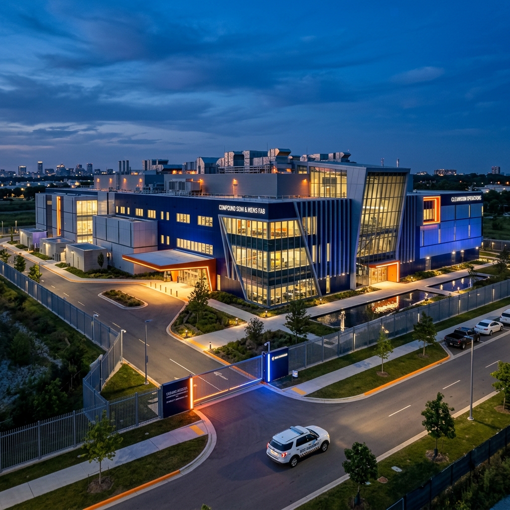
Compound Semiconductor & MEMS Fab
Physically isolated cleanroom for exotic materials (GaAs, InP) preventing cross-contamination. Utilizes DRIE to carve microscopic cavities for MEMS sensors.
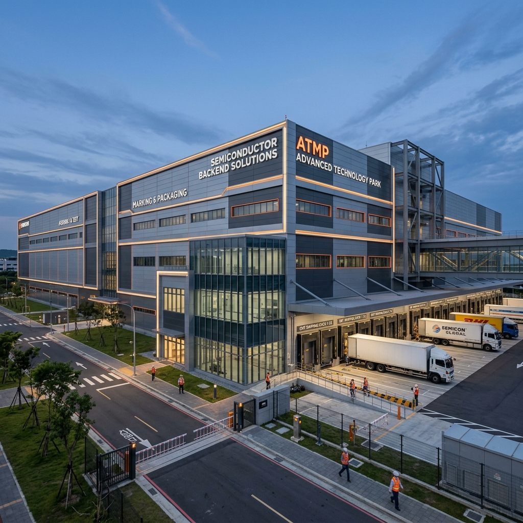
ATMP / SMT Backend Assembly
Captures value across the supply chain. Wafers are thinned, laser-diced, and packaged into finished, market-ready engine control units (ECUs) via PCBA.
Integrated Semiconductor
Mega-Fab Complex
A sovereign state-of-the-art facility engineered for sub-micron cleanrooms, bulk specialty chemical delivery, cryogenic storage, and vibration-isolated waffle slabs.
Facility Operations
Showcase
Step inside our manufacturing lines. Explore the high-fidelity metrology logs, precision metrics, and cleanroom hardware powering our output.
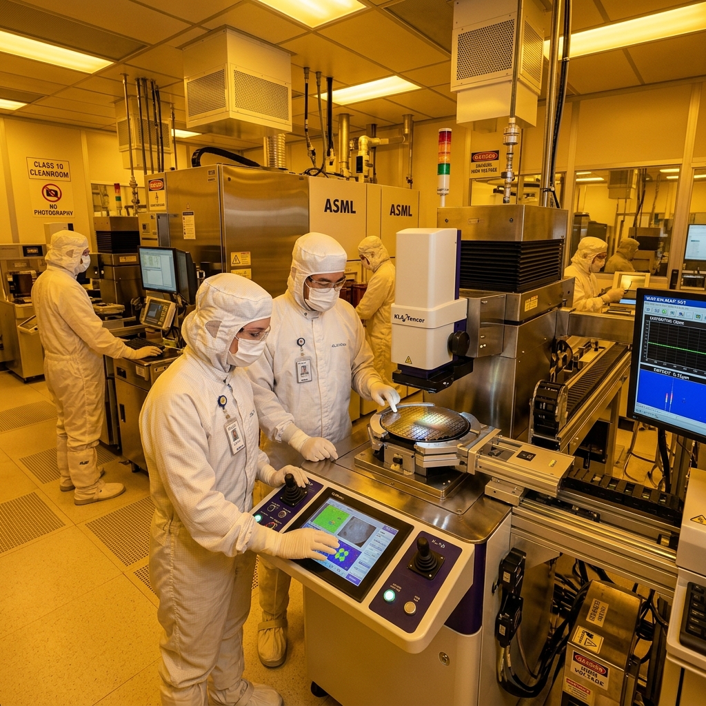
ISO Class 5 Cleanroom
Wafer fabrication cleanroom facility utilizing advanced ArF lithography systems and robotic wafer handling tracks.
Robotic SMT Assembly Lines
High-speed surface mount technology placing microscopic components on motherboards with sub-micron precision.
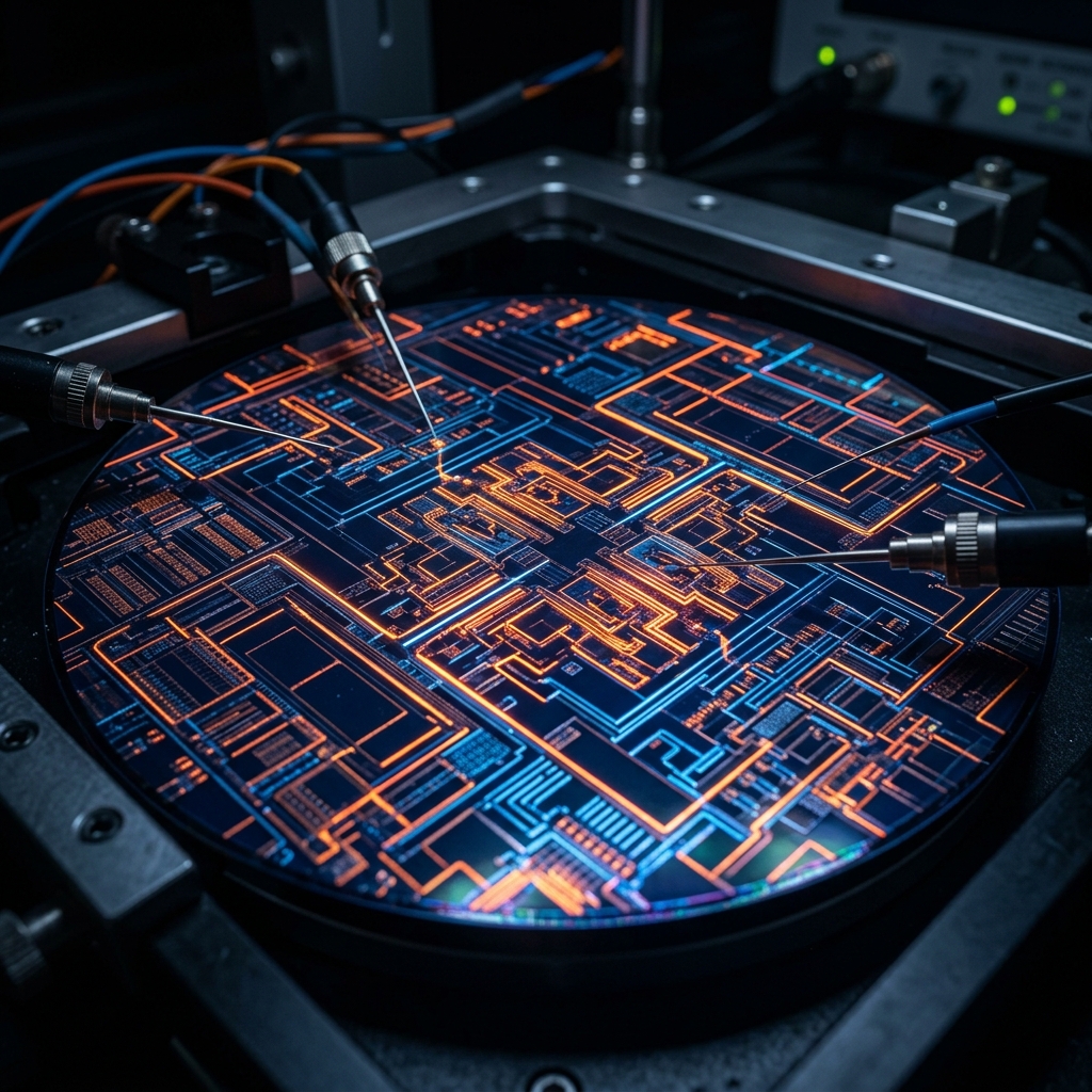
Wafer Probe Metrology
Macro silicon wafer testing under optical microscopes and ultra-fine probe cards to identify electrical node faults.
Advanced Chip Packaging
Microscopic wire-bonding micro-lenses attaching gold and copper wire traces to raw silicon core dies.
Scale That Speaks
Operating Divisions
Vertically integrated
Process Nodes
Silicon CMOS range
Planned Jobs
Employment target
Campus Size
Haringhata, WB
Operations
Round-the-clock
Investment (₹)
Phase 1 committed
World-Class
Capabilities
28nm – 180nm Silicon CMOS
Our silicon CMOS foundry delivers mixed-signal, RF, and power management ICs across mature and mid-range nodes. With industry-leading yield rates and a commitment to quality, every wafer that leaves our facility meets the highest standards.
Process Range
28nm – 180nm+
Wafer Diameter
200mm / 300mm
Lithography
ArF 193nm Dry
Yield Rates
Industry Leading
Responsible Manufacturing for a Greener India
Our commitment extends beyond silicon. Closed-loop water reclamation, rooftop & solar farm power, and zero-hazardous landfill policies are engineered directly into Bengal Mega-Fab.
85%
Water Recovery
Reclamation target
40%
Solar Power
Renewable energy share
90%
Zero Waste
Recycling rate
2035
Net-Zero
Carbon neutral target
GLOBAL CERTIFICATIONS & ALLIANCES
News & Insights
Top Semiconductor Companies in West Bengal & Kolkata: 2026 Ecosystem Guide & INDNIX Technology
Comprehensive 2026 guide to semiconductor companies in Kolkata and West Bengal: top 10 semiconductor companies, pure-play fab initiatives by INDNIX Technology Limited, talent pools, and career applications at the Kolkata cleanroom plant.
INDNIX vs TATA vs Foxconn: Indian Semiconductor Landscape, Chip Projects & Comparisons
In-depth strategic comparison of India's chip landscape: Who is bigger, INDNIX or TATA? Which is better, Foxconn or INDNIX? What was India's first chip, is there a chip shortage, and what are the top 10 semiconductor stocks in India?
INDNIX Semiconductor: Everything You Need to Know (Fab Plant, Stock Listing, CEO & Kolkata Careers)
Comprehensive public guide addressing top questions about INDNIX: Is INDNIX making semiconductors? Where is the fab plant located in West Bengal? Is INDNIX stock listed on NSE/BSE? Who is the CEO, and how to apply for semiconductor jobs in Kolkata?