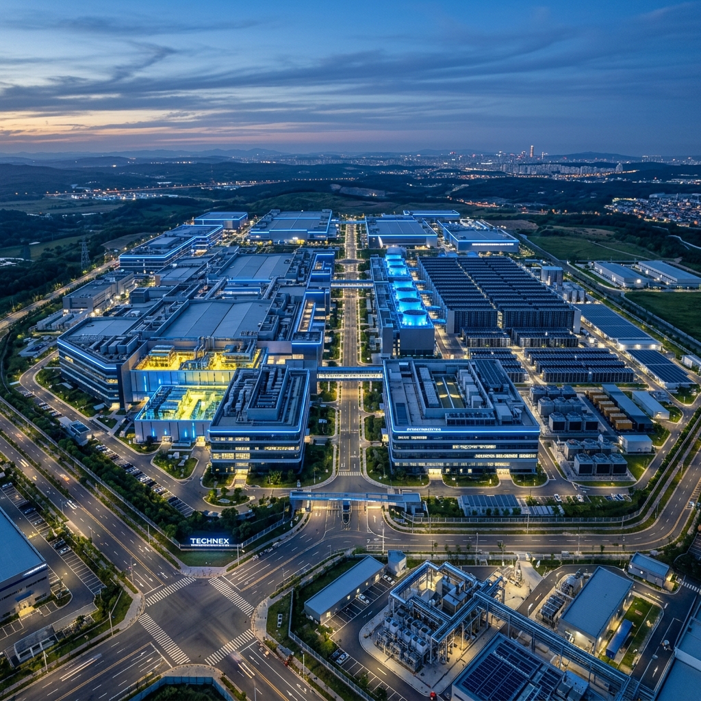
9 Integrated Divisions, One Campus
Assembly & Test, Compound Fab, RF, Power, Analog, IoT, Design, AI & Software — all under one roof.
Services & Capabilities
Seven integrated divisions spanning the complete semiconductor value chain — from design services to wafer fabrication and packaging.
0+
Operating Divisions
0–180nm
Process Nodes
0+
Planned Jobs
0 Acres
Campus Size
0/7
Operations
$0Billion
Investment (₹)
Technology Highlights
Cutting-edge semiconductor capabilities powering the next generation of electronics.
Quality & Certification
Every wafer and assembled unit undergoes rigorous metrology, electrical testing, and reliability qualification — meeting ISO, IATF, and AEC-Q100 standards.
Certifications
ISO 9001, 14001, IATF 16949
Testing
Burn-in, HTOL, ESD
Defect Target
< 0.1 DPPM
News & Insights
Latest technical articles, press releases, and industry perspectives from INDNIX.
INDNIX Proposes Mega-Fab to West Bengal State Government
INDNIX Technology Limited has proposed a comprehensive $1.5B USD mega-fab at the Bengal Silicon Valley Tech Hub, following a high-level meeting with State Government officials.
The Future of Advanced System-in-Package (SiP) Assembly
Explore how System-in-Package assembly is revolutionizing electronics by integrating multiple dies, passives, and sensors into a single compact module.
Overcoming Thermal Challenges in High-Density PCB Assembly
Learn the engineering strategies behind managing heat in densely populated PCB assemblies, from reflow profile optimization to advanced thermal interface materials.
Responsible Manufacturing for a Sustainable Future
Our commitment extends beyond silicon — water reclamation, renewable energy, and ethical supply chain practices are woven into every process.
Learn About Our Commitment85%
Water Reclamation
Recovery Target
40%
Renewable Energy
Power from Solar
90%
Waste Reduction
Recycling Rate
2035
Carbon Neutral
Net-Zero Target
Certifications & Affiliations