About Us
Corporate Relations
Contact our corporate relations desk for institutional partnerships and governance inquiries.
Contact Us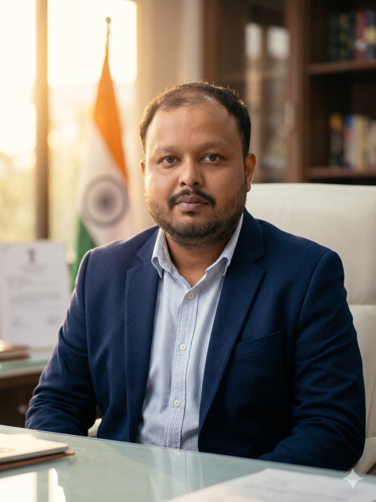
Soham Biswas
Chairman & Managing Director
Pioneering India’s Silicon Sovereignty
Dear Visitors, Partners, Investors, and Future Stakeholders,
Welcome to INDNIX Technology Limited.
You have arrived at the digital threshold of what I firmly believe is the most transformative industrial endeavor in the modern history of Eastern India. As you navigate through our corporate platform, you are not merely looking at a company profile; you are witnessing the blueprint of a national mission. We stand at the precipice of a new epoch—the Silicon Age of India.
For decades, the global economy has been powered by a resource that is smaller than a postage stamp yet infinitely more complex than any mechanical engine: the semiconductor. Today, integrated circuits and microprocessors are the lifeblood of modern civilization. They are the silent engines driving automotive electric vehicles (EVs), telecommunications, artificial intelligence, aerospace defense, and industrial automation. Yet, despite being a global powerhouse in software and chip design, India has historically remained heavily reliant on foreign imports for the physical manufacturing of these critical components. This dependency has exposed our sovereign supply chains to immense geopolitical vulnerabilities.
At INDNIX, we are answering the clarion call of our Hon'ble Prime Minister’s vision for an Aatmanirbhar Bharat (Self-Reliant India). We are transitioning India from a consumer of global silicon to a formidable architect of it.
The INDNIX Vision: Igniting a Regional Renaissance
Our vision is absolute: to build sovereign resilience in the global electronic value chain while simultaneously ending a three-decade-long industrial drought in Eastern India.
Located at the Haringhata Industrial Park in West Bengal, INDNIX is mobilizing a massive 35.40-acre campus that will serve as the beating heart of the Bengal Silicon Valley Tech Hub. For too long, the brilliant engineering minds forged in Eastern India’s premier academic institutions have had to migrate across the globe to find work at the cutting edge of deep-tech manufacturing. With INDNIX, we are bringing the frontier of global technology directly to Kolkata.
We are not just constructing a factory; we are cultivating a self-sustaining ecosystem. Operating a semiconductor facility requires an intricate web of electronic-grade chemical suppliers, ultra-pure raw material vendors, and high-precision logistics networks. By establishing this anchor mega-project, we will create a powerful ripple effect across India’s MSME landscape.
Furthermore, our commitment to human capital is unprecedented. INDNIX is projected to create over 7,000 direct, high-skilled engineering and technical jobs, alongside an estimated 450,000 indirect roles within the local economy over the next 48 months. By forging strategic partnerships with premier institutions like the Indian Institute of Engineering Science and Technology (IIEST), Shibpur, and Maulana Abul Kalam Azad University of Technology (MAKAUT), we are actively developing specialized "Dummy Cleanroom" training centers. We are building a robust talent pipeline that ensures our youth are "Fab-Ready" to take on the world.
The Investment: A $7.0 Billion CapEx Commitment to the Future
The scale of INDNIX is defined by uncompromising ambition and hardcore, multi-billion-dollar technical execution. We are currently architecting Eastern India’s first sovereign Integrated Semiconductor Mega-Fab with a projected Phase-1 Capital Expenditure of ₹58,100 Crores (approximately $7.0 Billion USD).
What separates INDNIX from conventional proposals is our vertically integrated approach. We are bridging the gap between raw wafer fabrication and finished hardware assembly under one unified corporate umbrella. Our Mega-Fab complex comprises three distinct, state-of-the-art divisions, engineered for a total throughput of 70,000 Wafer Starts Per Month (WSPM):
- The 28nm HKMG Silicon Logic Foundry: The cornerstone of our campus, focusing on 28nm High-K Metal Gate mature-node logic arrays, along with 45nm–180nm capabilities for RF and Power Management ICs. This facility will rely on highly proven, cost-effective equipment—including advanced ASML lithography platforms—to guarantee high-yield production for our fabless design clients.
- The III-V Compound Semiconductor & MEMS Fab: A highly specialized line dedicated to Gallium Arsenide (GaAs) and Indium Phosphide (InP) compound processing. This division will enable next-generation micro-scale sensing, catering to the exploding global demand for LiDAR, radar, and aerospace sensors.
- Advanced ATMP & SMT Operations: A high-volume Assembly, Testing, Marking, and Packaging (ATMP) backend, complete with Surface-Mount Technology (SMT) lines. Here, we package the raw silicon die into Advanced System-in-Package (SiP) architectures, delivering finished, market-ready microchips directly to global automotive and industrial OEMs.
To support this staggering capacity, our engineering and procurement teams are executing infrastructure on an "Ultra-Mega" scale. This includes deep-earth vibration-isolated waffle slabs required for nano-scale photolithography, ISO Class 2 cleanrooms, a Kinetic DRUPS flywheel microgrid to ensure zero-millisecond power drops, and an 18-Million Gallon per Day (MGD) Ultra-Pure Water (UPW) filtration plant.
Navigating Policy: The Bedrock of Financial Stability
A project of this magnitude cannot be realized in isolation; it requires the unwavering synergy of both Central and State Governments. INDNIX is uniquely positioned to leverage the most aggressive and supportive industrial policies in India’s history.
At the federal level, INDNIX is strictly aligned with the mandates of the Ministry of Electronics and Information Technology (MeitY) and the modified India Semiconductor Mission (ISM). Under the highly progressive Semicon 2.0 Policy, the financial architecture of our project is massively de-risked by substantial Central CapEx subsidies on a pari-passu basis. Specifically, our CMOS-based silicon fab is structured to be eligible for a 40% capital expenditure subsidy, while our compound semiconductor and advanced packaging (ATMP) units are structured for 35% financial support.
At the state level, the Government of West Bengal has demonstrated exceptional foresight and commitment to this industrial renaissance. We are actively engaged with the Chief Minister's Office and the Department of Finance to secure "Ultra-Mega Project Status." This status unlocks critical, customized fiscal incentives, including 100% exemptions on electricity duty for 10 years, 100% stamp duty waivers on our 35.40-acre land lease, and comprehensive SGST reimbursements. Furthermore, the State’s infrastructural guarantees—including the routing of a dedicated 220kV/400kV Extra-High Voltage (EHV) substation and raw water pipelines—ensure that our operational lifelines are secured against all bureaucratic bottlenecks.
This dual-engine backing from both New Delhi and Nabanna effectively bridges the financial gap, accelerating our path to profitability and ensuring that institutional capital is protected by sovereign guarantees.
An Invitation to Global Investors and Partners
To our prospective investors—Sovereign Wealth Funds, Private Equity syndicates, Venture Capitalists, and strategic corporate anchors—I offer a compelling proposition. Investing in INDNIX is not merely a financial transaction; it is a stake in the geopolitical realignment of the global technology supply chain.
The semiconductor foundry business is driven by capacity and predictability. We are aggressively securing Long-Term Wafer Supply Agreements (WSAs) with domestic fabless design startups and international automotive/heavy-machinery conglomerates (such as the ITL/Yanmar network). These pre-booked capacities, combined with the massive influx of non-dilutive government subsidies, provide a highly stabilized return on investment (ROI) profile that is rarely seen in deep-tech infrastructure projects.
Furthermore, we are calling upon the brightest minds in the industry. To the global Tier-1 semiconductor experts, expatriates, and process engineers currently working in Taiwan, Europe, and the United States: India is calling you home. We are building an executive leadership team and an engineering core that will command the respect of the global market. Bring your expertise to INDNIX, and help us calibrate the machines that will write the next chapter of technological history.
Commitment to the Future
As we move forward with the finalization of our Detailed Project Report (DPR) and the rigorous execution of our EPC master schedule, my pledge to you as Chairman and Managing Director is one of absolute transparency, unyielding quality, and relentless execution.
We understand the gravity of handling exotic materials and massive power loads, which is why we are implementing uncompromising Environmental, Health, and Safety (EHS) protocols, including a state-of-the-art Zero Liquid Discharge (ZLD) effluent treatment plant. We are building a facility that is not only technologically supreme but also ecologically sustainable.
The era of India sitting on the sidelines of hardware manufacturing is definitively over. From the smartphones in our pockets to the autonomous vehicles of tomorrow, the silicon that powers the future will be fabricated, tested, and packaged right here in West Bengal.
Thank you for your interest, your trust, and your partnership. Together, let us power the future. Let us build INDNIX.
Soham Biswas
Chairman & Managing Director
INDNIX Technology Limited